5.2 The WFC3 UVIS Channel CCD Detectors
5.2.1 Basics of CCD Operation
A charge-coupled device (CCD) is a silicon-based detector containing a two-dimensional array of summing wells called pixels, short for picture elements. Each pixel accumulates electric charge in proportion to the number of photons striking that location on the detector. Physically, the summing wells are created by electric fields established at the depletion (charge-free) regions of the Si-SiO2 metal-oxide-semiconductor (MOS) capacitors. In a typical three-phase CCD, the size of the depletion region is controlled by the voltage of three gates. The gates are arranged in parallel, with every third gate connected together.
At the end of an exposure, the voltages of the gates are changed with an appropriate clocking pattern, causing all charge packets to be sequentially transferred to the adjacent pixel, until they reach the readout circuitry at the detector’s edge. The transfer of charges between pixels occurs in parallel, row by row, whereas the extraction of the “zeroth” row at the edge occurs along an external serial register, where each packet is serially transferred to an output amplifier at the detector corner.
5.2.2 The WFC3 CCDs
The WFC3 UVIS channel uses two CCD detectors fabricated by Teledyne e2v.1 Both CCDs are 2051 × 4096 devices with 15 × 15 μm square pixels. There are 2051 rows by 4096 columns, where the row/column definition follows the convention of having the parallel direction first and the serial direction second. Having the serial register along the long (4096 pixel) edge reduces the number of transfers required to read out a charge packet.
The WFC3 CCDs are three-phase devices, thinned and back-illuminated (back-thinned) to improve the sensitivity to UV light. Thinning refers to the removal of the thick substrate on which the chip is originally built and is done to improve shorter-wavelength efficiency (only those electrons generated in the vicinity of the gate structure can be collected efficiently). Back-illumination means that photons are focussed on the back side of the chip, rather than having to pass through the opaque gate structures implanted on the front side.
Similar to ACS, the WFC3 CCDs also have buried channels and are operated in multi-pinned phase (MPP) mode. The purpose of the buried channel, or mini-channel, is to improve CTE for targets with relatively low signal levels (~10K e– or less) and reduce the dark current as well. The buried channels have the capability of injecting charges to fill in the traps and improve the CTE but this mode is not currently in use (Section 6.9.2). Further details of these features are given in Section 5.4.8.
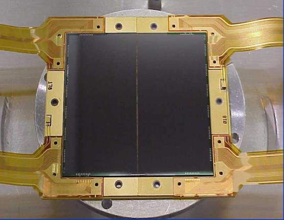
The two WFC3 CCDs are aligned together along their long dimension to create a 2 × 1 mosaic. This butted configuration is equivalent to a 4102 × 4096 array, but with a gap of 31 ± 0.1 pixels between the two chips (1.2 arcsec on the sky). Figure 5.1 shows a picture of a CCD assembly similar to the flight detector.
The CCDs are cooled by a four-stage thermoelectric cooler (TEC) to a nominal temperature of 190 K. The detectors are packaged inside a cold enclosure, which is nearly identical to the one used for ACS, itself a scaled-up version of the STIS design. The package includes a second cooled window to reduce the radiative heat load.
The CCD focal plane is assembled on a molybdenum base disk, which provides some shielding from cosmic rays and also serves as the thermal sink path from the hot side of the TEC stack to the heat pipes (which carry the heat to the external radiator). The “cover” with the external window is about 1 cm thick and is made of “alloy 42" steel; it provides some protection from cosmic rays incident on the front side of the CCDs.
The WFC3 CCDs are quite similar to those used in the ACS Wide Field Channel (WFC). They have the same pixel size, nearly the same format (2051 × 4096 in WFC3, compared to 2048 × 4096 in ACS), the same orientation of the serial and parallel registers, similar technology (buried-channel, MPP operation), and nearly identical mechanical interfaces. The main differences of the WFC3 chips compared to those in ACS/WFC are:
- UV optimization of the WFC3 wavelength response
- Significantly lower readout noise for the WFC3 chips (~3.1- 3.2 e– compared to 3.75-5.65 e–)
- 2051 rows instead of 2048
- Charge-injection capability for mitigation of degradation in CTE due to on-orbit radiation damage (not generally available for science observations; see Section 6.9.2)
- 31-pixel gap instead of 50
- Manufactured by Teledyne e2v from two separate wafers;1 ACS chips were produced by Site from the same wafer.
An overview of the WFC3 CCD performance was given in Table 5.1.
Figure 5.1: Detector package similar to the WFC3/UVIS flight detector. The size of the 4k × 4k array is approximately 6 × 6 cm, and it consists of two butted 2051 × 4096 CCDs with a 31-pixel gap between them.
1. The English Electric Valve Company (e2v, as it was known at the time) was acquired in 2017 by Teledyne Technologies.
-
WFC3 Instrument Handbook
- • Acknowledgments
- Chapter 1: Introduction to WFC3
- Chapter 2: WFC3 Instrument Description
- Chapter 3: Choosing the Optimum HST Instrument
- Chapter 4: Designing a Phase I WFC3 Proposal
- Chapter 5: WFC3 Detector Characteristics and Performance
-
Chapter 6: UVIS Imaging with WFC3
- • 6.1 WFC3 UVIS Imaging
- • 6.2 Specifying a UVIS Observation
- • 6.3 UVIS Channel Characteristics
- • 6.4 UVIS Field Geometry
- • 6.5 UVIS Spectral Elements
- • 6.6 UVIS Optical Performance
- • 6.7 UVIS Exposure and Readout
- • 6.8 UVIS Sensitivity
- • 6.9 Charge Transfer Efficiency
- • 6.10 Other Considerations for UVIS Imaging
- • 6.11 UVIS Observing Strategies
- Chapter 7: IR Imaging with WFC3
- Chapter 8: Slitless Spectroscopy with WFC3
-
Chapter 9: WFC3 Exposure-Time Calculation
- • 9.1 Overview
- • 9.2 The WFC3 Exposure Time Calculator - ETC
- • 9.3 Calculating Sensitivities from Tabulated Data
- • 9.4 Count Rates: Imaging
- • 9.5 Count Rates: Slitless Spectroscopy
- • 9.6 Estimating Exposure Times
- • 9.7 Sky Background
- • 9.8 Interstellar Extinction
- • 9.9 Exposure-Time Calculation Examples
- Chapter 10: Overheads and Orbit Time Determinations
-
Appendix A: WFC3 Filter Throughputs
- • A.1 Introduction
-
A.2 Throughputs and Signal-to-Noise Ratio Data
- • UVIS F200LP
- • UVIS F218W
- • UVIS F225W
- • UVIS F275W
- • UVIS F280N
- • UVIS F300X
- • UVIS F336W
- • UVIS F343N
- • UVIS F350LP
- • UVIS F373N
- • UVIS F390M
- • UVIS F390W
- • UVIS F395N
- • UVIS F410M
- • UVIS F438W
- • UVIS F467M
- • UVIS F469N
- • UVIS F475W
- • UVIS F475X
- • UVIS F487N
- • UVIS F502N
- • UVIS F547M
- • UVIS F555W
- • UVIS F600LP
- • UVIS F606W
- • UVIS F621M
- • UVIS F625W
- • UVIS F631N
- • UVIS F645N
- • UVIS F656N
- • UVIS F657N
- • UVIS F658N
- • UVIS F665N
- • UVIS F673N
- • UVIS F680N
- • UVIS F689M
- • UVIS F763M
- • UVIS F775W
- • UVIS F814W
- • UVIS F845M
- • UVIS F850LP
- • UVIS F953N
- • UVIS FQ232N
- • UVIS FQ243N
- • UVIS FQ378N
- • UVIS FQ387N
- • UVIS FQ422M
- • UVIS FQ436N
- • UVIS FQ437N
- • UVIS FQ492N
- • UVIS FQ508N
- • UVIS FQ575N
- • UVIS FQ619N
- • UVIS FQ634N
- • UVIS FQ672N
- • UVIS FQ674N
- • UVIS FQ727N
- • UVIS FQ750N
- • UVIS FQ889N
- • UVIS FQ906N
- • UVIS FQ924N
- • UVIS FQ937N
- • IR F098M
- • IR F105W
- • IR F110W
- • IR F125W
- • IR F126N
- • IR F127M
- • IR F128N
- • IR F130N
- • IR F132N
- • IR F139M
- • IR F140W
- • IR F153M
- • IR F160W
- • IR F164N
- • IR F167N
- Appendix B: Geometric Distortion
- Appendix C: Dithering and Mosaicking
- Appendix D: Bright-Object Constraints and Image Persistence
-
Appendix E: Reduction and Calibration of WFC3 Data
- • E.1 Overview
- • E.2 The STScI Reduction and Calibration Pipeline
- • E.3 The SMOV Calibration Plan
- • E.4 The Cycle 17 Calibration Plan
- • E.5 The Cycle 18 Calibration Plan
- • E.6 The Cycle 19 Calibration Plan
- • E.7 The Cycle 20 Calibration Plan
- • E.8 The Cycle 21 Calibration Plan
- • E.9 The Cycle 22 Calibration Plan
- • E.10 The Cycle 23 Calibration Plan
- • E.11 The Cycle 24 Calibration Plan
- • E.12 The Cycle 25 Calibration Plan
- • E.13 The Cycle 26 Calibration Plan
- • E.14 The Cycle 27 Calibration Plan
- • E.15 The Cycle 28 Calibration Plan
- • E.16 The Cycle 29 Calibration Plan
- • E.17 The Cycle 30 Calibration Plan
- • E.18 The Cycle 31 Calibration Plan
- • E.19 The Cycle 32 Calibration Plan
- • E.20 The Cycle 33 Calibration Plan
- • Glossary