5.5 The WFC3 IR Channel Detector
5.5.1 Overview
The infrared channel of WFC3 employs a low-noise, high-QE, 1024 × 1024 pixel HgCdTe array manufactured by Teledyne Imaging Sensors (formerly Rockwell Science Center). The detector area sensitive to light is 1014 × 1014 pixels. Active cooling by a six-stage thermoelectric cooler (TEC) keeps the detector at a nominal operating temperature of 145 K. Although the IR detector is sensitive between 400 and 1700 nm, the detector coating is optimized for wavelengths longward of ~1000 nm, where the QE peaks (Figure 5.25). The IR channel filter set is also limited to wavelengths above 900 nm, making the IR channel complementary to the UVIS channel.
Compared to CCD detectors, IR detectors like the one used in the WFC3 IR channel have higher read noise and dark current. Unlike CCDs, however, IR detectors allow the accumulated signal in each pixel to be measured non-destructively multiple times. The capability to sample the signal multiple times during the integration can be exploited to reduce the effective read-out noise significantly as well as to remove cosmic rays. IR exposures are called “ramps” due to this capability to sequentially read the detector as signal accumulates. IR detectors are also immune to the charge bleeding exhibited by CCDs at high signal levels. Saturation is still a concern, however, because pixels subject to the highest signal levels show higher dark-current rates (“image persistence” or afterglow) in subsequent exposures (WFC3 ISR 2010-17). Section 7.9.4 discusses the on-orbit characterization of persistence on the WFC3/IR detector, and Appendix D summarizes ways to plan observations to minimize the impact of persistence.
The capability of multiple readouts and the absence of bleeding makes IR detectors able to perform very high dynamic-range observations. Non-destructive readouts also allow for the recovery of pixels affected by cosmic rays (CRs), because CR hits can be recognized and removed between adjacent reads. Unlike CCDs, IR detectors show minimal long-term on-orbit CTE degradation because they do not employ the charge transfer mechanism used in CCDs. IR detectors, however, are intrinsically non-linear. Nevertheless, at low and intermediate signal levels, the departure from linearity is quite modest and can be well calibrated by a low-order polynomial fit, whose parameters can in principle be determined for each pixel.
5.5.2 IR Detector Basics
In this section, we briefly describe the operational principles of the WFC3/IR detector. Figure 5.20 (adapted from McLean 1997, Electronic Imaging in Astronomy: Detectors and Instrumentation) shows the basic physical structure of the photovoltaic HgCdTe detector used in WFC3.
Figure 5.20: Cross-section of a WFC3/IR detector (not to scale).
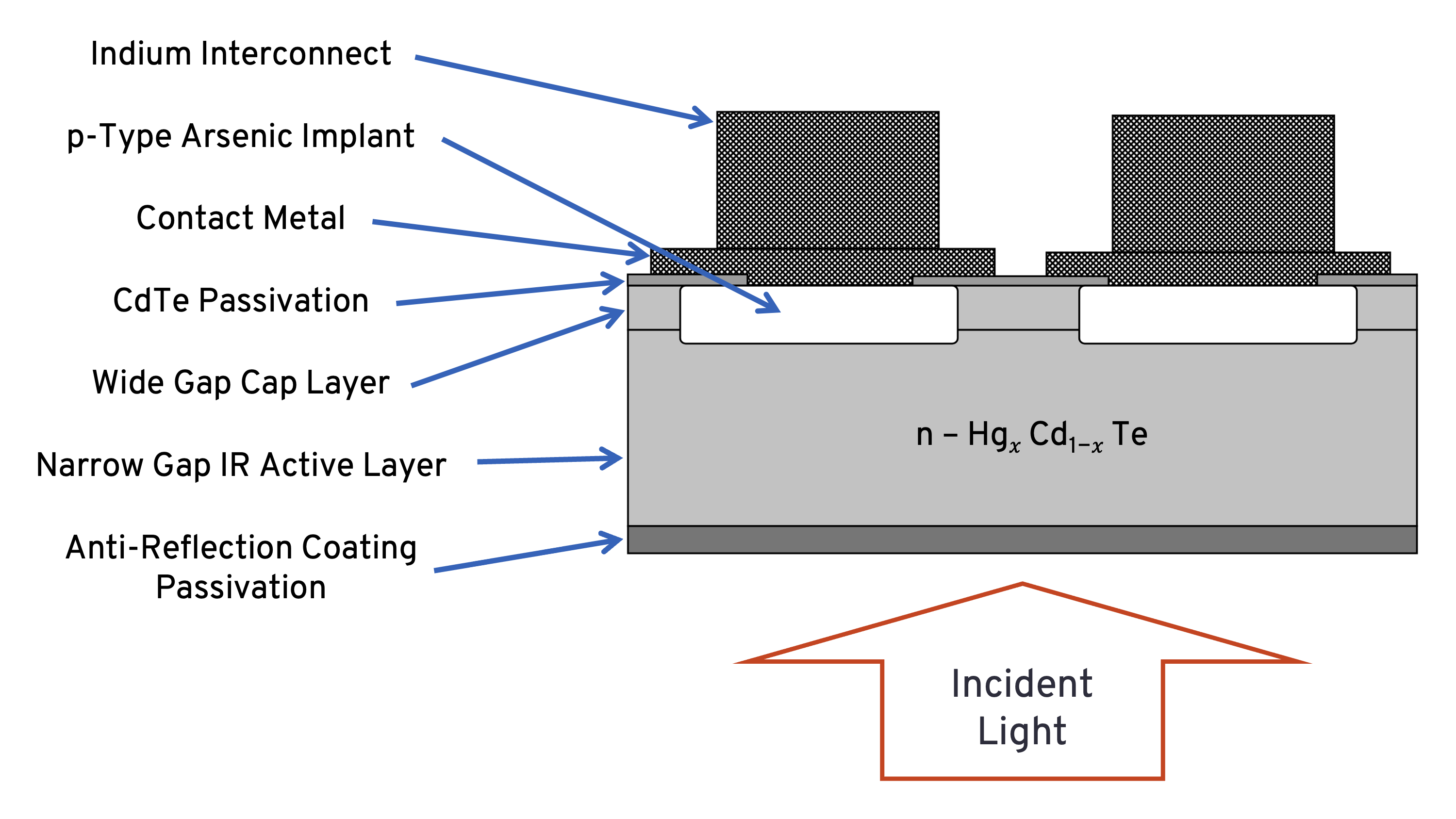
Infrared detectors used in astronomy today are basically two-dimensional arrays of p-n junctions working as photodetectors (photodiodes). In a p-n junction, negative charges migrate from the n-type doped material to saturate the unmatched covalent bonds of the adjacent p-type material. The displaced carriers establish an electric field across the junction, setting up an intermediate region depleted of free carriers. The depletion region is therefore both charged and highly resistive. The strength of the electric field and the size of the depletion region may be increased by applying an external electric field (“negative bias”). This biasing corresponds to the initial RESET applied at the beginning of an IR ramp. When an incident IR photon is absorbed by the photosensitive material, it creates a free electron-hole pair. The two photo-generated charges drift in the material and would eventually recombine. However, if the mobility of the charge carrier (a hole in an n-type material) is high enough, it will reach the depletion region before recombining and be swept to the other side of the junction by the electric field. There, in the p-type region, it will recombine with one of the electrons of the ionized holes, causing a reduction of the voltage across the junction. This change of voltage can be measured and, being proportional to the number of photo-generated charges, provides a direct measure of the photons captured on each pixel.
In the case of the WFC3 IR detector, the photosensitive material is made of HgCdTe grown with a molecular beam epitaxial (MBE) process on a ZnCdTe substrate. The fraction of Hg vs. Cd controls the long-wavelength cutoff of the material, whereas the doping material (As for the p-type, In for the n-type) creates the p-n junction. The MBE growth process is different from that used in the NICMOS detectors on HST, in which the HgCdTe was grown on sapphire in a liquid phase (PACE process). MBE growth on a ZnCdTe substrate is expected to provide a better lattice match to HgCdTe than sapphire, creating fewer defects and charge traps at the interface between the two materials. The MBE growth process is followed by the processing phase, in which the implants and contacts of each pixel are manufactured.
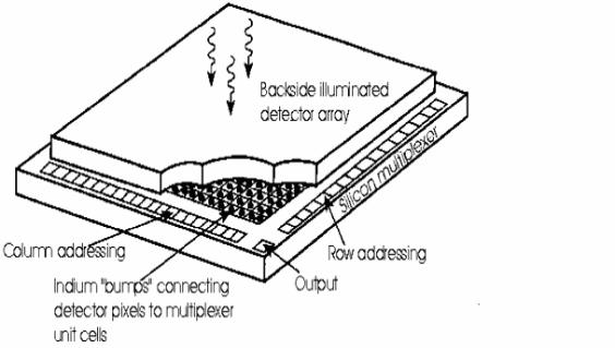
As usual with IR arrays, the readout circuitry is made on a separate CMOS chip (multiplexer or MUX), which is eventually hybridized to the detector with an indium contact for each pixel (Figure 5.21). After the two chips have been hybridized, the ZnCdTe substrate is removed to reduce the susceptibility of the device to cosmic-ray events which also increases the sensitivity at short wavelengths. The final chip therefore is a CMOS device connected through indium columns to a thin layer of HgCdTe photosensitive material.
Figure 5.21: Basic “hybrid” structure of infrared array detectors (not to scale).
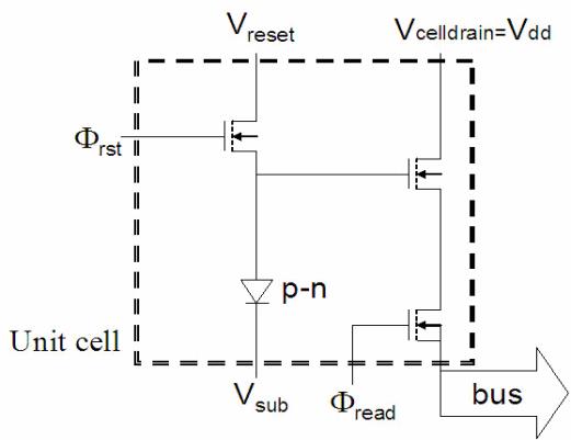
In the MUX, each pixel has its own dedicated readout circuitry (unit cell). In particular, the voltage change across the p-n junction is monitored by a field-effect transistor (FET) configured as a source-follower amplifier, which has gain of 1 and effectively decouples the detection process from the noisy readout circuitry. Two other FETs connect the pixel to the reset voltage and the output line. Figure 5.22 shows the equivalent circuit diagram for the WFC3 detector unit cell. Each WFC3/IR unit cell contains three transistors. For comparison, the NICMOS detectors had four transistors, whereas the latest generation of Hawaii-2RG detectors for JWST has seven transistors per unit cell. A higher number of transistors increases the versatility of the device. For example, on the NICMOS detectors it is possible to reset each individual cell, whereas on WFC3 detectors the reset is sent simultaneously to all cells on the same row. Note that since there are no potential barriers between pixels, pixels do not spill charges into nearby pixels when they reach a certain level (“blooming full well”) of accumulated charges, as in typical multiphase CCDs. Therefore, IR detectors do not show “bleeding” along columns. Moreover, due to individual readout, bad pixels do not block the rest of the column as they do in a CCD.
Figure 5.22: Equivalent circuit diagram of the WFC3/IR unit cell.
-
WFC3 Instrument Handbook
- • Acknowledgments
- Chapter 1: Introduction to WFC3
- Chapter 2: WFC3 Instrument Description
- Chapter 3: Choosing the Optimum HST Instrument
- Chapter 4: Designing a Phase I WFC3 Proposal
- Chapter 5: WFC3 Detector Characteristics and Performance
-
Chapter 6: UVIS Imaging with WFC3
- • 6.1 WFC3 UVIS Imaging
- • 6.2 Specifying a UVIS Observation
- • 6.3 UVIS Channel Characteristics
- • 6.4 UVIS Field Geometry
- • 6.5 UVIS Spectral Elements
- • 6.6 UVIS Optical Performance
- • 6.7 UVIS Exposure and Readout
- • 6.8 UVIS Sensitivity
- • 6.9 Charge Transfer Efficiency
- • 6.10 Other Considerations for UVIS Imaging
- • 6.11 UVIS Observing Strategies
- Chapter 7: IR Imaging with WFC3
- Chapter 8: Slitless Spectroscopy with WFC3
-
Chapter 9: WFC3 Exposure-Time Calculation
- • 9.1 Overview
- • 9.2 The WFC3 Exposure Time Calculator - ETC
- • 9.3 Calculating Sensitivities from Tabulated Data
- • 9.4 Count Rates: Imaging
- • 9.5 Count Rates: Slitless Spectroscopy
- • 9.6 Estimating Exposure Times
- • 9.7 Sky Background
- • 9.8 Interstellar Extinction
- • 9.9 Exposure-Time Calculation Examples
- Chapter 10: Overheads and Orbit Time Determinations
-
Appendix A: WFC3 Filter Throughputs
- • A.1 Introduction
-
A.2 Throughputs and Signal-to-Noise Ratio Data
- • UVIS F200LP
- • UVIS F218W
- • UVIS F225W
- • UVIS F275W
- • UVIS F280N
- • UVIS F300X
- • UVIS F336W
- • UVIS F343N
- • UVIS F350LP
- • UVIS F373N
- • UVIS F390M
- • UVIS F390W
- • UVIS F395N
- • UVIS F410M
- • UVIS F438W
- • UVIS F467M
- • UVIS F469N
- • UVIS F475W
- • UVIS F475X
- • UVIS F487N
- • UVIS F502N
- • UVIS F547M
- • UVIS F555W
- • UVIS F600LP
- • UVIS F606W
- • UVIS F621M
- • UVIS F625W
- • UVIS F631N
- • UVIS F645N
- • UVIS F656N
- • UVIS F657N
- • UVIS F658N
- • UVIS F665N
- • UVIS F673N
- • UVIS F680N
- • UVIS F689M
- • UVIS F763M
- • UVIS F775W
- • UVIS F814W
- • UVIS F845M
- • UVIS F850LP
- • UVIS F953N
- • UVIS FQ232N
- • UVIS FQ243N
- • UVIS FQ378N
- • UVIS FQ387N
- • UVIS FQ422M
- • UVIS FQ436N
- • UVIS FQ437N
- • UVIS FQ492N
- • UVIS FQ508N
- • UVIS FQ575N
- • UVIS FQ619N
- • UVIS FQ634N
- • UVIS FQ672N
- • UVIS FQ674N
- • UVIS FQ727N
- • UVIS FQ750N
- • UVIS FQ889N
- • UVIS FQ906N
- • UVIS FQ924N
- • UVIS FQ937N
- • IR F098M
- • IR F105W
- • IR F110W
- • IR F125W
- • IR F126N
- • IR F127M
- • IR F128N
- • IR F130N
- • IR F132N
- • IR F139M
- • IR F140W
- • IR F153M
- • IR F160W
- • IR F164N
- • IR F167N
- Appendix B: Geometric Distortion
- Appendix C: Dithering and Mosaicking
- Appendix D: Bright-Object Constraints and Image Persistence
-
Appendix E: Reduction and Calibration of WFC3 Data
- • E.1 Overview
- • E.2 The STScI Reduction and Calibration Pipeline
- • E.3 The SMOV Calibration Plan
- • E.4 The Cycle 17 Calibration Plan
- • E.5 The Cycle 18 Calibration Plan
- • E.6 The Cycle 19 Calibration Plan
- • E.7 The Cycle 20 Calibration Plan
- • E.8 The Cycle 21 Calibration Plan
- • E.9 The Cycle 22 Calibration Plan
- • E.10 The Cycle 23 Calibration Plan
- • E.11 The Cycle 24 Calibration Plan
- • E.12 The Cycle 25 Calibration Plan
- • E.13 The Cycle 26 Calibration Plan
- • E.14 The Cycle 27 Calibration Plan
- • E.15 The Cycle 28 Calibration Plan
- • E.16 The Cycle 29 Calibration Plan
- • E.17 The Cycle 30 Calibration Plan
- • E.18 The Cycle 31 Calibration Plan
- • E.19 The Cycle 32 Calibration Plan
- • E.20 The Cycle 33 Calibration Plan
- • Glossary