5.4 WFC3 CCD Characteristics and Performance
5.4.1 Quantum Efficiency
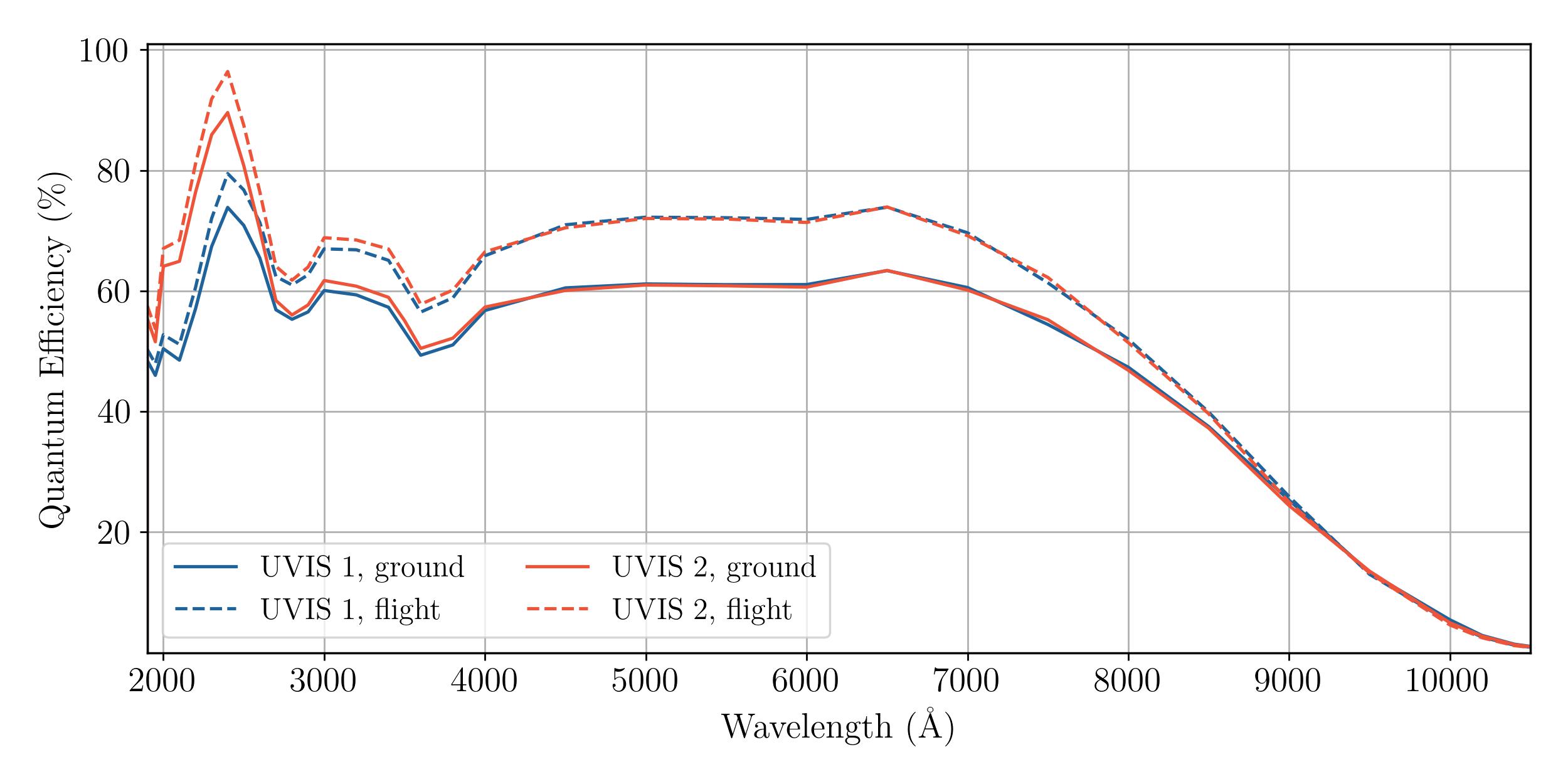
The quantum efficiencies (QEs) of the two WFC3 CCDs are plotted against wavelength in Figure 5.2. Here the QE is defined as electrons yielded per incident photon. The solid curves illustrate the QEs as measured at the Detector Characterization Laboratory (DCL) at Goddard Space Flight Center, slightly corrected downward by the TV3 ground tests. The plots demonstrate the high sensitivity of the CCDs in the UV down to 200 nm. On the other hand, the peak QE at ~600 nm is less than that of the ACS/WFC detectors (~85% at their peaks). The QE measurements were made with the detectors perpendicular to the incident light. As installed in WFC3, the CCDs are tilted by 21 degrees with respect to the normal. The nominal change in optical thickness is ~6%, but the QE variations, as measured at the DCL on similar devices, turn out to be negligible.
The integrated system throughput of WFC3 depends on many factors including the HST OTA, pickoff mirror, filter transmission functions, QE, etc. Based on ground measurements of these components, the intergrated system throughput was calculated and compared to the first on-orbit measurements during Servicing Mission/Orbital Verification in 2009. A 5 to 20% increase in the integrated system throughput was discovered, likely attributable to multiple components. The dashed curves represent the QE under the assumption that the entire flight correction is in the detector QE. For UV observations, UVIS2 achieves a higher sensitivity than UVIS1.
Figure 5.2: Quantum efficiency curves of the WFC3 UVIS 1 (blue) and UVIS 2 (orange) CCDs based on Goddard DCL measurements corrected by TV3 measurements (solid). The integrated system throughput of the UVIS detector was measured on-orbit to be higher than ground tests by 5–20%, and the dashed curves shows the QE under the assumption that this entire gain is due to the QE. In reality, some fraction of this gain is likely attributable to other HST and/or instrument components.
5.4.2 Multiple-Electron Events at Short Wavelengths
Like the ACS HRC and STIS CCDs (and unlike WFPC2), the WFC3 UVIS CCDs are directly sensitive to UV photons. In silicon, photons of energy higher than 3.65 eV (i.e., wavelength shorter than ~340 nm) can produce multiple electron-hole pairs when the energetic conduction-band electron collides with other valence-band electrons. At higher energies (energy above 3.65 eV, or wavelength below ~340 nm) the incident photons can directly extract more than one electron from the valence band. This effect (called “quantum yield”) of a single photon producing more than one electron must be taken into account properly when estimating the noise level for short-wavelength observations.
Because the generation of multiple electrons is a random phenomenon, an extra noise term must be added to account for an observed variance larger than that associated with the normal Poisson distribution of incoming photons. The correction is theoretically about 1.7 e–/photon at 200 nm, decreasing linearly to 1.0 at 340 nm. Measurements of ground-based data, however, have indicated that the effect in the WFC3 chips is much less, 1.07 e–/photon at 218 nm and 1.03 e–/photon at 275 nm in broadband data (WFC3 ISR 2008-47) as well as monochromatic narrowband data (WFC3 ISR 2010-11). The cause for this is unclear, but may be due to charge sharing (Janesick, J.R., 2007, “Photon Transfer DM-->λ“, SPIE, Bellingham, Washington, p 45-48).
Given the low level of quantum yield measured in the WFC3 data, neither the QE curves presented in Figure 5.2 nor the WFC3 Exposure Time Calculator (ETC) include the effects of quantum yield. The noise distortion from multiple electrons is not large compared to other contributions to the signal-to-noise ratio in the ultraviolet (see Section 9.2).
5.4.3 Flat Fields
Before launch, ground-based flats were obtained for all UVIS filters at an SNR of ~200 per pixel using an external optical stimulus (WFC3 ISR 2008-12). Because the overall illumination pattern of the ground-based flats did not precisely match the illumination attained on-orbit from the OTA, there are errors in these ground-based flats on large spatial scales. These errors were quantified by performing stellar photometry on rich stellar fields that were observed using large-scale dither patterns during SMOV and Cycles 17-18 (2009-2011). In the on-orbit SMOV exposures, calibrated with the ground-based flats, the RMS difference between the average magnitude of a star and its magnitude in the first pointing varied from 1.5% to 4.5%, from the long to the short wavelengths (WFC3 ISR 2009-19).
The needed corrections to the ground-based flats are now well understood, including the treatment of expected window ghosts (see WFC3 ISR 2011-16 and Section 6.5.3). New reference files were delivered for all UVIS filters except the QUAD filters in December 2011 (WFC3 ISR 2013-10). The goal was to support photometry to ~1% accuracy over the full WFC3 UVIS field of view for most of the broadband filters (F336W, F390W, F438W, F555W, F606W, F775W, F814W), and to 2-3% accuracy for the remaining filters, for apertures of radius 0.4 arcsec. The actual accuracies of these flat fields were assessed via observations of bright HST standard stars on different portions of the detector in 8 filters to quantify any spatial variability in the photometry (WFC3 ISR 2015-18). For the UV filters, photometric residuals due to the crosshatch pattern in the flats (an artifact of the chip manufacturing process; see Figure 5.3) were found to be 1.8% rms and 6.7% peak-to-peak. Color differences between the blue HST standards and the average color of Omega Cen, which was used to compute inflight corrections to the ground flats, were found to account for offsets in the UV photometry of up to 5% between the two UVIS chips. Based on this analysis, an improved set of flat fields was generated and delivered to the HST archive to support the new chip-dependent calibration implemented in calwf3 version 3.3 in February 2016 (see Section E.2).
A complete description of the new chip-dependent flat fields is given in WFC3 ISR 2016-04. Flats were computed using the TV3 ground flats and corrected for a large internal reflection or flare that arises due to the expected window ghosts (WFC3 ISR 2011-06). L-flats (low-frequency corrections to the ground flats) were derived from dithered observations of stars in the Omega Cen cluster, and account for low-frequency variations in sensitivity over the detector field of view. The three key differences of the 2016 set of flat field reference files with respect to the prior (2011) set are:
- The star cluster observations were corrected for CTE (Charge Transfer Efficiency) effects before computing the L-flat;
- The L-flat solutions were computed from photometry of stars dithered across a single chip only (i.e. they now exclude stars dithered between chips); and
- The flats were independently normalized using the median value for each chip, rather than a small region on amplifier A. This changed the normalization by less than 1% for filters with pivot wavelengths longer than 400 nm.
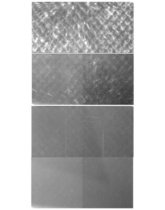
The new UV flats are based on ground test data obtained in ambient conditions, and have been corrected for the ~3% sensitivity variations that correlate with a crosshatch pattern (on scales of 50 - 100 pixels) seen in the flats at short wavelengths. Figure 5.3 shows examples of bias-corrected ground-based flats for two wide-band filters. Both are displayed with an inverse greyscale stretch chosen to highlight features; the vignetting in the upper-right corner is not instrument-related but an artifact of the ground test optical stimulus. The crosshatch features in the UV flat field (F336W) are normal, due to the detection-layer structure in the CCDs; the level is typically <5% peak-to-peak compared to the rest of the flat.
During the time between anneals (when the UVIS detector is temporarily warmed; see Section 5.4.9), reductions in sensitivity ~1% to several percent develop in some pixels, especially at the bluer wavelengths (WFC3 ISR 2014-18). Reductions greater than 2-3% are rare in F438W and F814W (0.1% of the pixels), but occur in 3-10% of the pixels in F225W. About 90% of these pixels recover during an anneal, but the more strongly affected pixels can require more than one anneal to recover. Dithering of observations can mitigate the effect.
The latest information about UVIS flats can be found on the WFC3 UVIS Flats webpage. |
Figure 5.3: WFC3/UVIS ground-based flat fields at F336W (top) and F555W (bottom).
5.4.4 Long-Wavelength Fringing
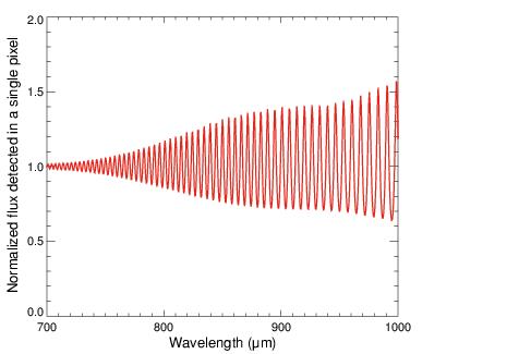
Multiple reflections between the layers of a CCD detector can give rise to fringing, where the amplitude of the fringes is a strong function of the silicon detector layer thickness and the spectral energy distribution of the light source. Like most back-thinned CCDs, the WFC3 CCDs exhibit fringing at wavelengths longward of ~600-700nm (see Figure 5.4). The amplitude of the flat-field signal for monochromatic input increases gradually with wavelength and can reach levels of ± 50% at the longest CCD wavelengths (fringe amplitude is the envelope of the curve shown in Figure 5.5).
An analysis of fringing effects in broadband-illuminated ground flats longward of 600nm (WFC3 ISR 2010-04) has shown that F953N has the greatest fringe amplitude (~16%), followed by the quad filters FQ889N, FQ906N, FQ924N, and FQ937N (~10%). Other narrowband and quad filters have fringe amplitudes in the range of 0.5-4.6% (F656N, F658N, FQ672N, F673N, FQ674N, FQ727N, and FQ750N). Although fringing is generally weak at wavelengths shorter than 700 nm, the very narrow H-alpha filter (F656N) exhibits a fringe amplitude of up to several percent in flat fields acquired during ground testing (WFC3 ISRs 2008-17, 2008-46 and 2010-04).
Note, however, that the amplitudes of fringing listed here (and in WFC3 ISR 2010-04) should be used only as an estimate of the effect in science data. Fringing will be different for sources with spectral energy distributions (SEDs) which differ significantly from the calibration lamp used to generate the ground flat fields. For example, continuum sources in broad filters will effectively smooth out fringing effects, but that same filter can show strong fringes when illuminated by sources with strong spectral lines or SEDs much narrower than the filter bandpass. Conversely, for sources with SEDs similar to the calibration lamp, the fringes can be corrected by the flat-fielding process.
The fringe pattern has been shown to be very stable, as long as the wavelength of light on a particular part of the CCD stays constant, so fringing can be corrected if an appropriate flat field is available. The fringe pattern can also be modeled, either by interpolating between or combining monochromatic patterns previously obtained in the laboratory, or from theoretical calculations. For a detailed explanation of efforts to model the WFC3 fringe pattern, see Malumuth et al. (2003, Proceedings of SPIE 4854, Future EUV/UV and Visible Space Astrophysics Missions and Instrumentation, pp. 567–576) and “Fringing in the WFC3/UVIS Detector”, presented by M. Wong at the 2010 STScI Calibration Workshop.
Figure 5.4: UVIS chip 1 (top) and chip 2 (bottom) fringe pattern for monochromatic illumination at 977 nm.
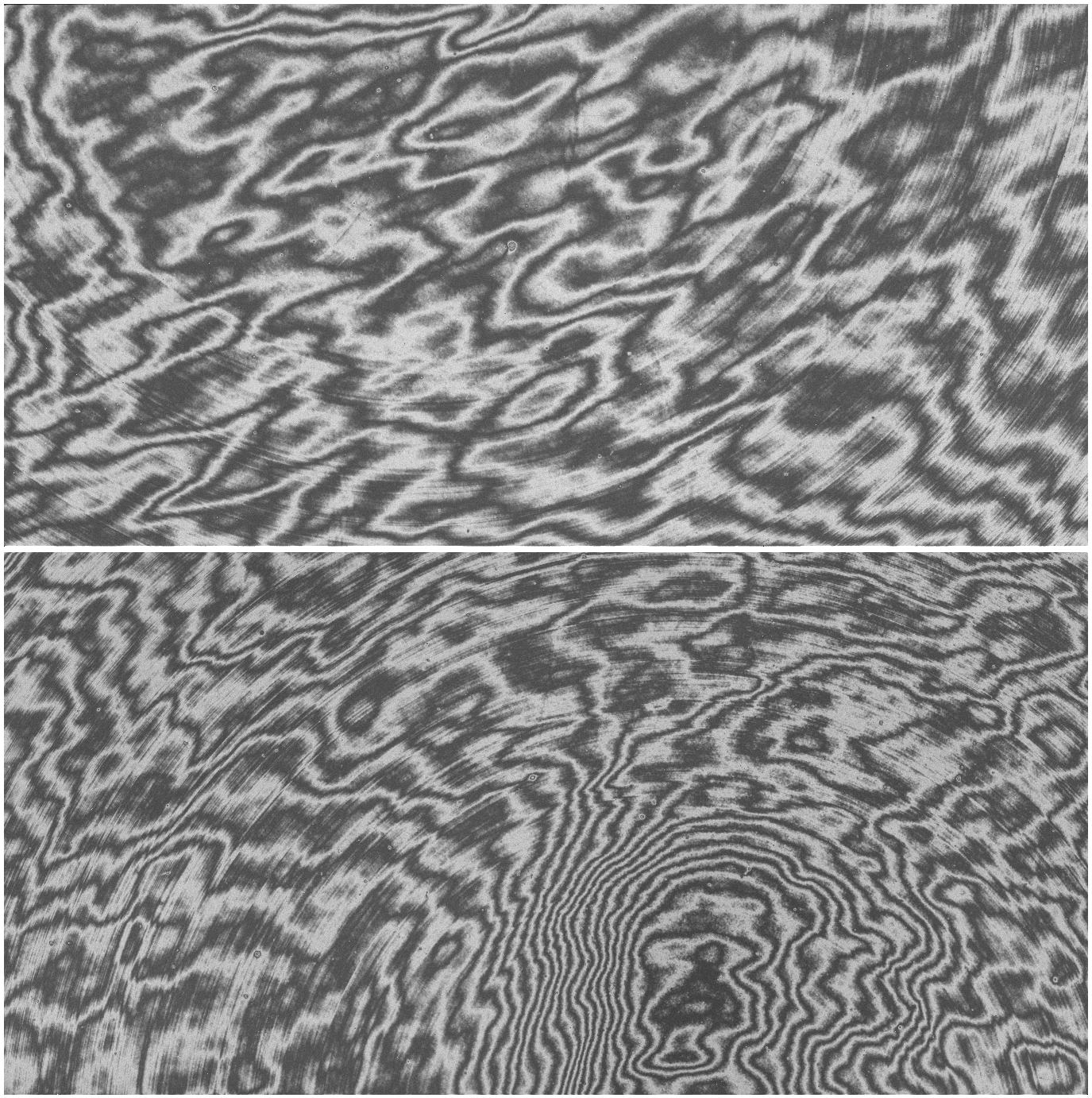
Figure 5.5: Flux (normalized to the mean of the image) as a function of wavelength for a single pixel, based on the Malumuth et al. (2003) model. Fringe phase (rapid oscillation) and fringe amplitude (curve envelope) vary as a function of wavelength. Due to wavelength averaging (even within narrow band filter bandpasses), actual WFC3 data exhibit peak to trough fringe amplitudes of < 30%.
5.4.5 Linearity and Saturation
The dynamic range of a detector is limited either by the full-well capacity of the device or by the analog-to-digital converter (ADC) and gain setting that are used during readout to convert the accumulated charge into data numbers (DN). At the standard UVIS gain of ~1.5 e⁻/DN, saturation always occurs on chip unless binning is used, in which case the effective saturation level is set by the 16-bit ADC rather than by the physical pixel full well. Because on-chip binning sums the charge from multiple physical pixels before digitization, the combined signal reaches the ADC limit (~65,535 DN) well before any pixel approaches its intrinsic full-well capacity. Consequently, accurate photometry of bright sources cannot be reliably recovered in binned UVIS data once the ADC limit is reached. See Section 5.4.6 for the numerical limits on DN and electrons for unbinned and binned readouts. Although the calibration pipeline continues to apply full-well saturation flagging to binned images for consistency, these flags have no practical meaning because ADC saturation always occurs first.
If saturation occurs on-chip, photometric information can still be recovered with reasonable accuracy, as described below. If the charge accumulated in a given readout pixel exceeds the ADC maximum, any additional charge does not result in a further increase in the DN and may, in cases of extreme saturation, result in values of zero. Extreme over-exposure is not expected to cause any long-term damage to the CCDs, so there are no bright-object limits for the WFC3 CCDs.
On-orbit PSF measurements show that the onset of saturation (i.e. the full-well depth where charge begins to spill along columns) in the WFC3/UVIS detectors varies by ~13% across both CCDs, from 63,400 to 72,400 e⁻ depending on location. Beginning with calwf3 v3.7.1, a new spatially varying saturation map introduced in WFC3 ISR 2025-06, has replaced the prior use of a constant threshold of 65,500 e⁻ in the calibration pipeline. The distribution of full-well depth on the detector is shown in Figure 5.6. This map is applied in the calibration pipeline for both full-frame and subarray UVIS exposures. For binned exposures, the ADC limit is reached first, so the full-well map does not determine the effective saturation level. Once the charge exceeds the pixel full-well level, it can escape that pixel and spread into adjacent vertical pixels; as the signal continues to accumulate, these adjacent pixels themselves can accumulate charge up to full well and leak into further adjacent vertical pixels, resulting in the “blooming,” or charge overflow, effect. The multi-phased pinned (MPP; see Section 5.4.8) operation of the detectors, used to minimize surface dark current, constrains the blooming along the detector columns, so the blooming is only vertical and not horizontal. Photometric information well beyond saturation can be recovered for relatively isolated sources in unbinned images by defining a special aperture that encompasses all of the pixels that contain the bloomed charge. WFC3 ISR 2010-10 presents an algorithm that can be invoked for UVIS1 to regain full linearity to ~1% up to nearly 7 magnitudes past saturation. UVIS2 is linear with simple summation over the saturated pixels. Some small non-linearities (a few percent) have been detected at the lowest signal levels at greater distances from the amplifiers, but the behavior is consistent with CTE loss (Section 5.4.11) rather than a true non-linearity in the chips.
The saturation map matches the state of the data at the stage of calwf3 where saturation flagging is applied. As a result, the effective full-well value for each pixel in each filter that corresponds to saturation may differ slightly from this map once all calibrations have been applied. For example, each filter has a unique flat-field calibration that effectively raises or lowers the number of raw counts across the detector. For these reasons, the saturation flags in the Data Quality (DQ) arrays should be used to determine whether or not a pixel is saturated. For saturated pixels the accumulated flux is non-linear with exposure time.
Figure 5.6: Distribution of full-well depth (in electrons) for UVIS1 (top half) and UVIS2 (bottom half). This map was derived using the fitting procedure described in WFC3 ISR 2025‑06, based on RAW PSF cutouts from external observations obtained since WFC3’s installation in 2009. This file, provided through CRDS, has been processed for calwf3 use by converting to units of electrons, applying bias subtraction, and including overscan regions to match the state of the data at which saturation flagging is applied.
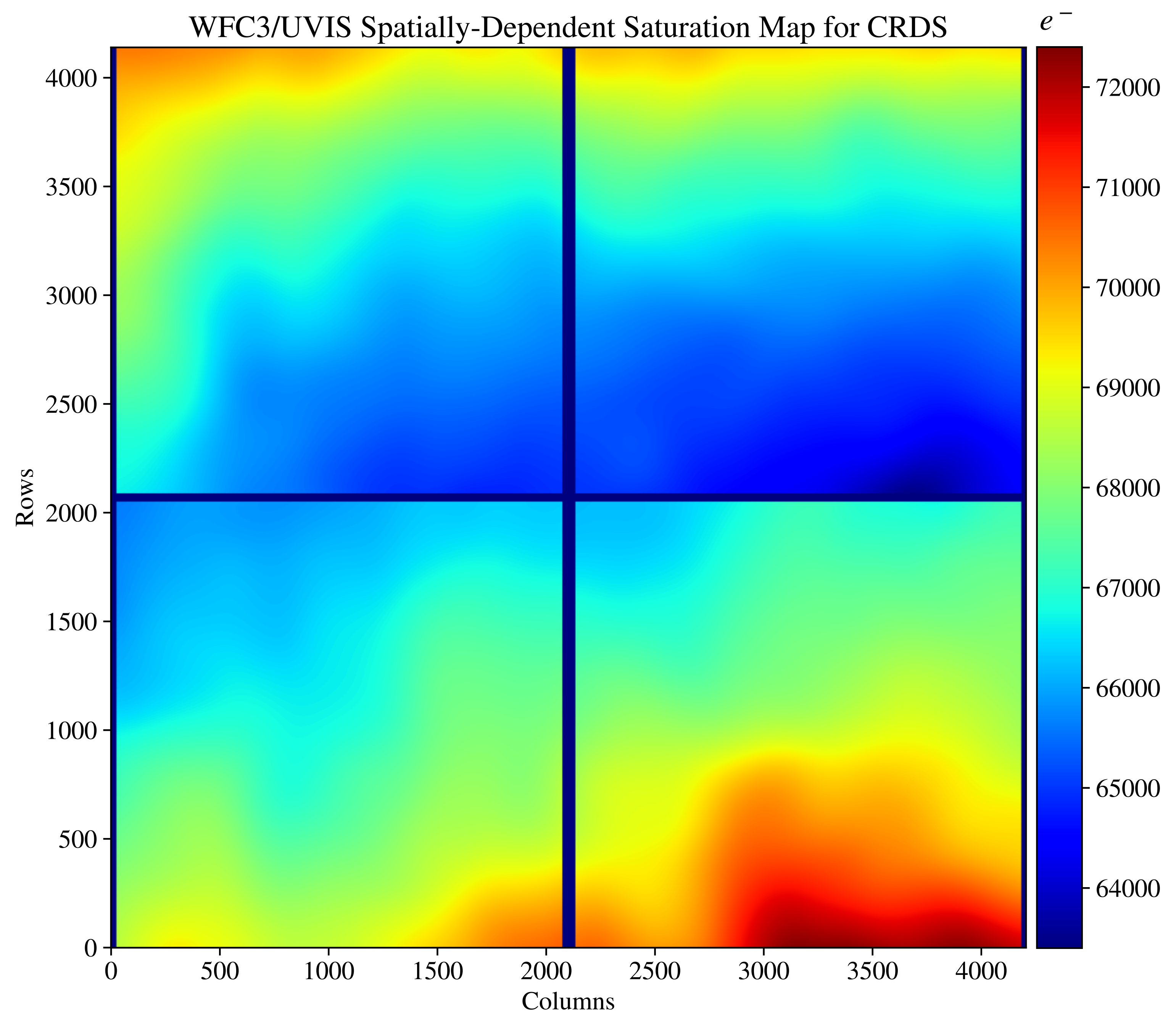
The saturation map reference file shown in Figure 5.6 is available for download directly from CRDS. The original map, derived from the fitting procedure prior to any modifications for calwf3, can be downloaded from the WFC3/UVIS Full Well Depth webpage. |
5.4.6 Gain
Electrons that accumulate in the CCD wells are read out and converted to data numbers (DNs), often called Analog-to-Digital Units (ADUs), by the analog-to-digital converter (ADC). The conversion gain is defined as the number of electrons required to produce one DN. The ADC output is a 16-bit number, limiting the maximum DN that can be read out to 216 - 1 or 65,535 for each readout pixel (single or binned detector pixel). Setting the conversion gain to unity, where one DN corresponded to one electron, would make it impossible to measure signals larger than 65,535 electrons. Adjusting the gain somewhat higher, so that multiple counts correspond to a single DN, allows larger numbers of electrons to be measured; however, the gain must also be low enough that it provides adequate sampling of the read noise.
For WFC3/UVIS, the default gain has been set to ~1.5 e–/DN. The maximum full well depth of the pixels on the WFC3/UVIS chips is ~72,400 e– (Figure 5.6), which at the default gain corresponds to ~48,000 DN, well below the ADC limit of 65,535 DN. If the pixels are binned 2 × 2 or 3 × 3, the binned pixels could reach flux levels of 4 or 9 times 48,000 DN, respectively, which would be truncated to 65,535 DN (~98,300 e–) during readout. Although it is possible to operate the WFC3 CCD detector at gains of ~ 1, 1.5, 2, and 4 e–/DN, only the gain of ~1.5 e–/DN is supported. For unbinned readouts, this gain permits sampling of the entire dynamic range of the detectors, with negligible impact on the readout noise.
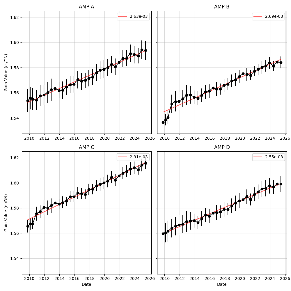
The on-orbit measured gain values for the WFC3 CCDs as of September 2025 are presented in Figure 5.7 and summarized in Table 5.3. The gain is increasing slightly with the age of the detector, partially due to CTE degradation, but remains consistent over time to within 1-2%.
Table 5.3: WFC3/UVIS Gain Values, as of September 2025.
CCD Chip | Amp | Gain (e–/DN) |
1 | A | 1.593 |
B | 1.584 | |
2 | C | 1.615 |
D | 1.599 |
Figure 5.7: Gain stability measurements across all four amplifiers from October 2009 to September 2025, following the procedure used in WFC3 ISR 2022-08.
5.4.7 Read Noise
The read noise level in the science area pixels of bias frames for all of the amplifiers at the default gain setting was measured in 2009 during SMOV (WFC3 ISR 2009-26). Table 5.4 shows the results obtained at the default gain setting of 1.5 e–/DN. The read noise was found to be stable to 1%, 0.4%, 0.7%, and 0.8%, for amps A,B,C, & D, respectively, based on measurements through the end of August 2009. The read noise is monitored on a monthly cadence using full-frame UVIS bias images. An analysis of long-term trends showed the read noise increased by 0.06-0.075 electrons (0.01 electrons/year from 2009 to 2017; WFC3 ISR 2017-17).
Trend appear to be stable with no deviations or sudden changes. The increase in read noise is attributed to the on-going CTE degradation as well as a growing number of hot pixels; see Section 6.9 for more details.
Table 5.4: WFC3/UVIS readout noise (e–) and uncertainty for normal and binned modes in 2009.
Amplifier A | Amplifier B | Amplifier C | Amplifier D | ||||||||||||
Binning | 1 × 1 | 2 × 2 | 3 × 3 | 1 × 1 | 2 × 2 | 3 × 3 | 1 × 1 | 2 × 2 | 3 × 3 | 1 × 1 | 2 × 2 | 3 × 3 | |||
Mean | 2.91 | 3.11 | 3.22 | 2.99 | 3.15 | 3.26 | 2.90 | 2.99 | 3.09 | 3.01 | 3.29 | 3.38 | |||
Uncertainty | 0.03 | 0.02 | 0.04 | 0.01 | 0.01 | <0.01 | 0.02 | <0.01 | 0.01 | 0.02 | 0.02 | <0.01 | |||
Analysis of the statistical behavior of the WFC3 ADCs showed some tendency for the least significant bit to be slightly biased at the readout speed adopted by the WFC3 electronics (WFC3 ISR 2005-27). However this effect is minor and does not degrade the photometric and noise characteristics of the WFC3/UVIS images.
5.4.8 Dark Current
The WFC3 CCDs, like most large-area scientific CCDs, operate with buried channels. Earlier generations of CCDs worked with surface channels, i.e., storing and transferring charges only along the surface of the semiconductor material. In these earlier devices, the Si-SiO2 interface between the detector material Si (p-doped conductor) and the surface layer of SiO2 (isolator) created significant charge traps, which limited both the charge transfer efficiency and the dark current (current measured without incident flux). In buried-channel devices, a shallow (~0.5 micron thick) n-type Si layer is implanted just below the surface between the p-doped Si and the SiO2 surface, to store and transfer the collected signal charge away from the traps at the interface.
Dark current in WFC3 detectors is further reduced using MPP (multi-phased pinned) technology. The dark current generated at the Si-SiO2 interface ultimately depends on two factors: the density of interface states and the density of free carriers (holes and electrons) that populate the interface. Electrons can thermally “hop” from the valence band to an interface state (sometimes referred to as a “mid-band state”) and from there to the conduction band, producing a dark electron-hole pair. Free carriers also fill interface states and, if these states were completely populated, can suppress hopping and conduction, reducing the surface dark current at levels comparable to the bulk dark. Unfortunately, normal CCD operations deplete the interface of free carriers, maximizing dark current generation.
In MPP technology, the Si-SiO2 interface is populated with holes that suppress the hopping conduction process. MPP mode is applied to the CCD by significantly biasing the array clocks negatively to invert (push electrons away from) the n-buried channel and “pin” the surface potential beneath each phase to substrate potential (hence the name multi-pinned phase). Biasing the array clocks in this manner causes holes from the p+ channel stops to migrate and populate the Si-SiO2 interface, eliminating surface dark-current generation. Note that it is not possible to invert conventional CCDs in this way, as the sensor's full-well capacity would be annihilated since the potential wells within a pixel all assume the same level. To circumvent this difficulty in MPP CCD technology, an additional implant is included below one of the phases, allowing charge to accumulate in collecting sites when biased into inversion.
Besides eliminating surface dark current, MPP CCD technology offers additional advantages. For example, the charge transfer efficiency of a CCD generally degrades with decreasing operating temperature. MPP technology assists in the charge transfer process because it permits the use of higher operating temperatures.
The MPP CCD also eliminates residual image, a serious problem that has plagued low-signal-level CCD users for many years. Residual image, also known as quantum-efficiency hysteresis, results when the sensor is either overexposed or first powered up. Under these circumstances, electrons trapped at the Si-SiO2 interface are slowly released into the pixel's potential well. Residual charge may take hours or even days before its level falls below the read-noise floor. Inverting the CCD causes holes to recombine immediately with the trapped residual electrons, eliminating remnant image effects during integration as well as readout.
During pre-flight tests, the CCD dark current was measured both in the cryogenic environment at the DCL, and in the instrument during thermal vacuum testing. The dark current levels have been regularly evaluated, e.g. during the 2004 thermal vacuum testing (WFC3 ISR 2005-13), early after installation in HST (WFC3 ISR 2009-16), and since then (WFC3 ISR 2014-04; WFC3 ISR 2016-08; WFC3 ISR 2019-10).
Like all CCDs operated in a low-earth-orbit radiation environment, the WFC3 CCDs are subject to radiation damage by energetic particles trapped in the radiation belts. Ionization damage and displacement damage are two types of impairment caused by protons in silicon. The MPP mode is very effective in mitigating the damage due to ionization, such as the generation of surface dark current due to the creation of new trapping states in the Si-SiO2 interface. Although protons lose only a minor fraction of their total energy via non-ionizing energy loss, lattice displacement damage can cause significant performance degradation in CCDs by decreasing the charge transfer efficiency (CTE), increasing the average dark current, and introducing pixels with very high dark current (hot pixels). Displacement damage to the silicon lattice occurs mostly due to the interaction between low-energy protons and silicon atoms. The generation of phosphorous-vacancy centers introduces an extra level of energy between the conduction band and the valence band of the silicon. As described above, new energy levels in the silicon bandgap increase the dark current as they allow thermally generated charges to reach the conduction band. As a consequence, the dark current of CCDs operated in a radiative environment is predicted to increase with time.
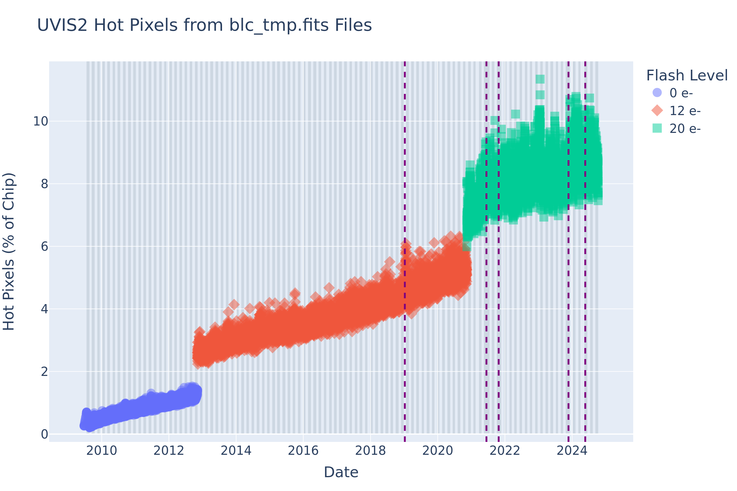
The measured dark current, defined as the median level of the pixels below the hot pixel threshold (defined as 54 e-/hr), is shown in Figure 5.8. As expected, due to radiation damage the dark current has been slowly increasing over time. In November 2012, post-flash became available for use to reduce CTE losses by increasing the image background (Section 5.4.11). As a result, the measured dark current levels dropped (WFC3 ISR 2014-04): with post-flash, CTE losses are reduced, which in turn reduces the flux trailed out from hot pixels and cosmic ray hits due to delayed release of electrons, thereby decreasing the dark current as well as increasing the measured number of hot pixels (Section 5.4.9). Later, in November 2020, the post-flash level was increased from 12 to 20 e-/pixels to compensate for continuing CTE losses, resulting in another slight reduction in the measured dark current (and increase in hot pixels).
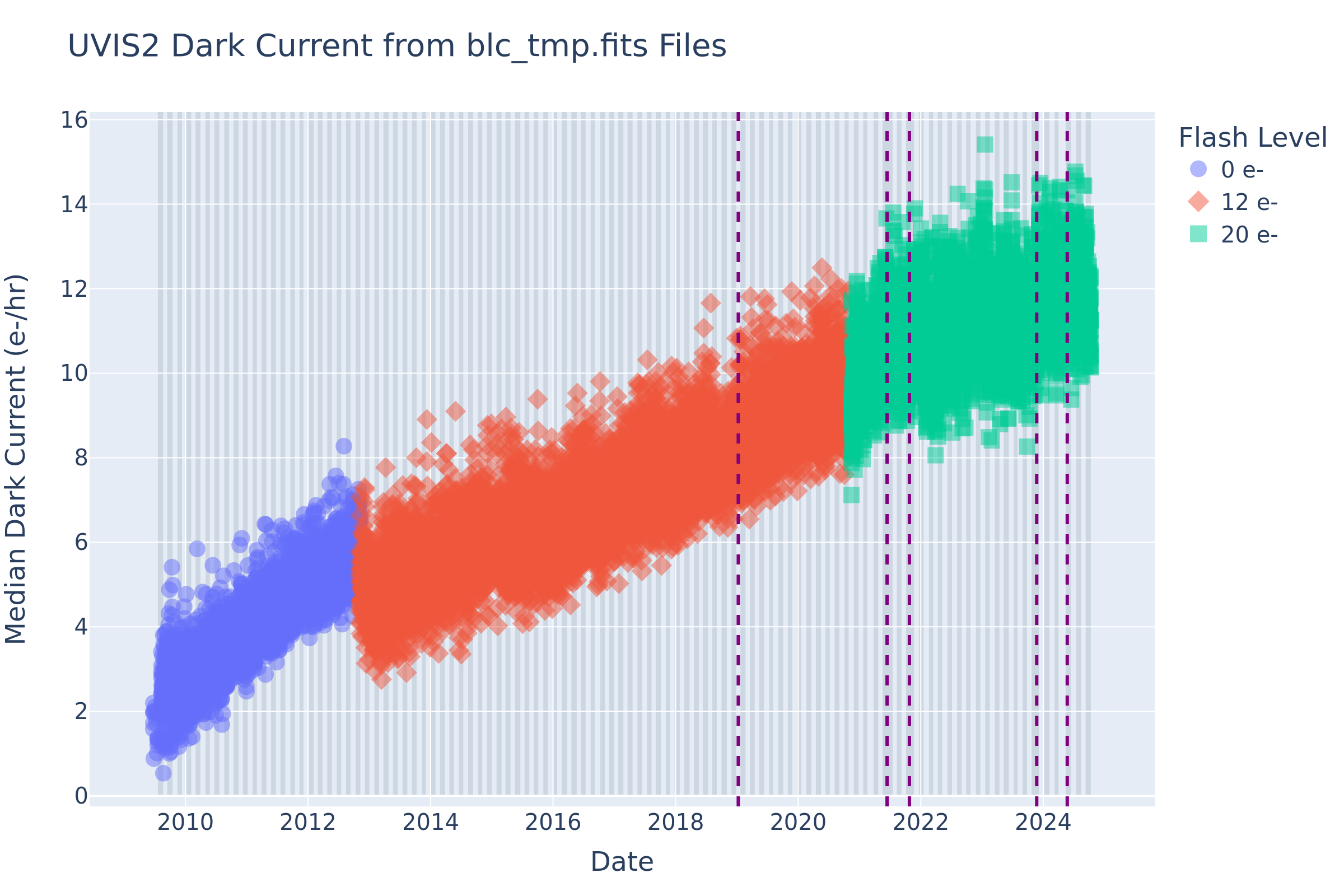
As of February 2016, with the introduction of calwf3 version 3.3 into the calibration pipeline, CTE-corrected images and calibration files have been produced (WFC3 ISR 2016-08). The CTE correction helps return electrons that have trailed out of their original pixel back to the pixels they came from, which allows for a more accurate measurement of the dark current and hot pixel levels. The result is a further reduction in median dark current and a smaller dispersion than for darks without a CTE correction (compare Figure 5.9 versus Figure 5.8). The rate of increase is also somewhat less than for darks without a CTE correction and there is an increase in the measured number of hot pixels at that time (Section 5.4.9).
Reference file darks made from unflashed and flashed dark exposures have been analyzed to better quantify the effects of post-flash on the dark pixel population and the hot pixel population (WFC3 ISR 2019-10).
Figure 5.8: Median dark current (e-/hr) of the WFC3/UVIS CCD 2 detector measured on orbit from June 2009 to October 2024, for non-CTE corrected darks ("blv_tmp" FITS files). Points are color-coded by post-flash levels for UVIS dark frames. Light and dark gray vertical shading indicates the monthly anneal periods. Vertical dashed lines mark some of the HST safing events within the past five years.
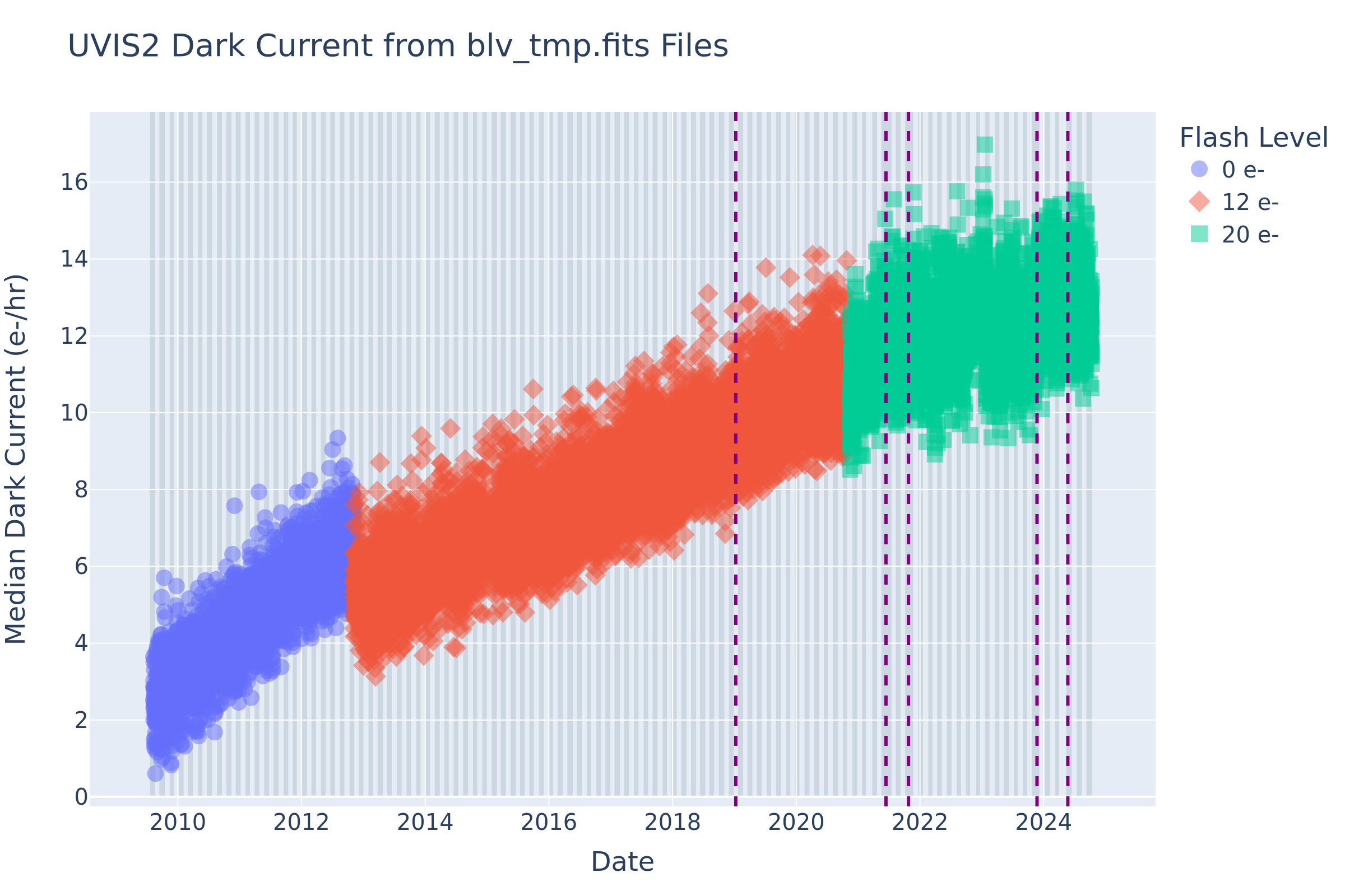
Figure 5.9: Median dark current of the WFC3/UVIS CCD 2 detector measured on orbit from June 2009 to October 2024, for CTE-corrected darks ("blc_tmp" FITS files). Points are color-coded by post-flash levels for UVIS dark frames. Light and dark gray vertical shading indicates the monthly anneal periods. Vertical dashed lines mark some of the HST safing events within the past five years.
5.4.9 Bad Pixels
Three types of bad pixels are routinely monitored using on-orbit WFC3 data: hot pixels (higher than normal dark current), bad detector pixels (unstable, often with extremely low quantum efficiency), and sink (charge trap) pixels and their associated trails. All these pixels are flagged in the DQI array of the calibrated data with values 16, 4, and (since Feb 2016 with the installation of calwf3 version 3.3) 1024, respectively (see also Appendix E and WFC3 ISR 2014-19).
On orbit, the number of hot pixels increases with time due to radiation damage, but is periodically partially reduced by annealing, when the UVIS detector is temporarily warmed to ~20°C. The number of sink pixels also grows over time, presumably because they are radiation-induced. Unlike hot pixels, sink pixels appear to be unaffected by anneals. The extent of the sink pixel CTE trail to be flagged is based on the science image background: the lower the background is, the longer the sink pixel trail will be (WFC3 ISR 2014-19, WFC3 ISR 2014-22).
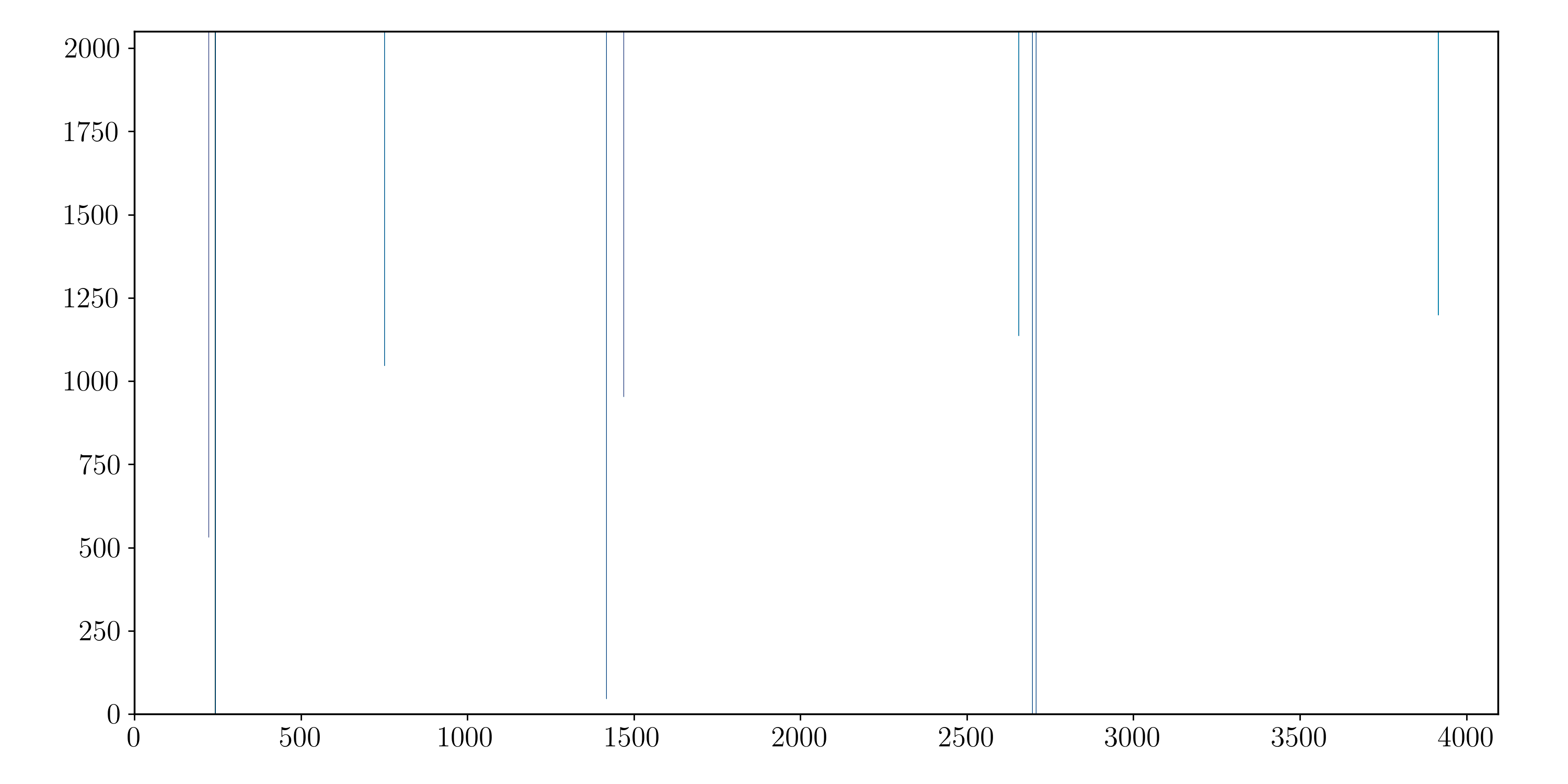
The bad detector pixel population, generally located along columns, is relatively constant. Bad detector pixels are shown for the upper chip (chip 1) and lower chip (chip 2) in Figure 5.10 and Figure 5.11, respectively. Note that a pair of bad columns passes near the center (reference pixel) of the subarray aperture UVIS2-C512C-SUB, which is at [282, 257] in the lower left corner of chip 2.
Figure 5.10: Bad detector pixels (DQI = 4) on the upper chip (chip 1) are in columns 1104, 2512, 2542, 2543, 2869, 3646, and 3667 in the flt image.
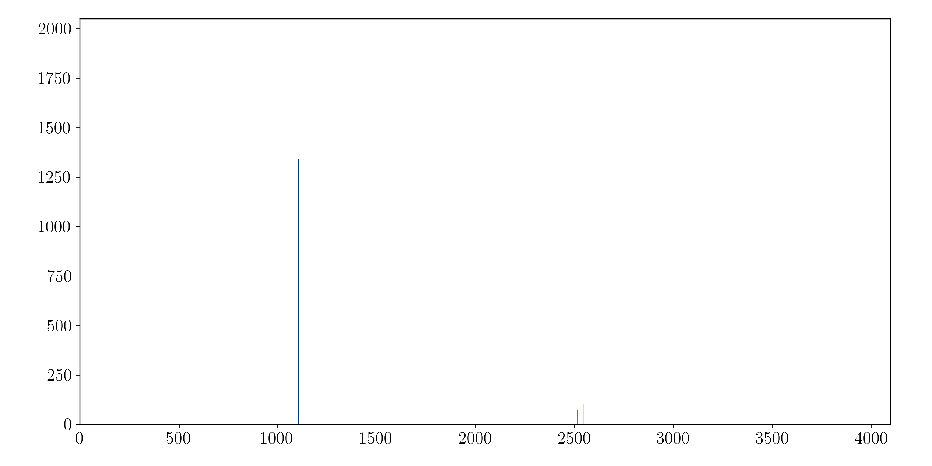
Figure 5.11: Bad detector pixels (DQI = 4) on the lower chip (chip 2) are in columns 223, 242, 243, 751, 1417, 1469, 2655, 2696, 2707, and 3915 in the flt image.
calwf3 pipeline (see WFC3 ISR 2016-08 for more information on superdarks). The impact of on-orbit radiation damage can be seen in the increase in hot pixels between the three different times; radiation damage also produces an increase in dark current as well (see Section 5.4.8). The vertical line at 54 e-/hr (13.5 e-/pixel) represents the previously-implemented hot pixel threshold, which was based on the tail of the dark current distribution and 900-second dark frames from 2009. For data from 2012-2020, when post-flash levels were at 12 e-/pixel, the UVIS bad pixel table pipeline used the 13.5 electron threshold.After increasing post-flash from 12 to 20 electrons in June 2020 to better mitigate CTE losses (WFC3 ISR 2020-08; WFC3 ISR 2021-03; WFC3 ISR 2021-06), it was observed that this ultimately led to a significant percentage of stable pixels being misflagged as unstable. To correct for this, in 2021 the WFC3 team implemented a formula into the pipeline to determine the hot pixel threshold; this formula is dependent on the post-flash level and dark current on the detector, and thus ensures a more accurate measurement of the unstable pixel population that is independent of future modifications to post-flash configurations (WFC3 ISR 2021-14).
Figure 5.12: Superdark histograms illustrate the increase in the number of hot pixels (>54 e–/hr) between anneal procedures. The March 31, April 11, and April 26 curves (red, green, and blue, respectively) are from 1-3 days after the anneal procedure, about mid-way between anneals, and about 1-3 days prior to the next anneal procedure.
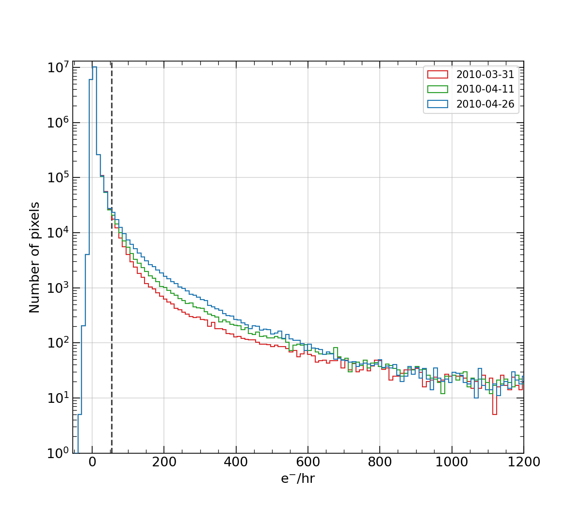
Figure 5.13: Hot pixel growth for the WFC3/UVIS CCD 2 detector between anneals from June 2009 to October 2024, as measured from non-CTE-corrected darks ("blv_tmp" FITS files). Points are color-coded by post-flash levels for UVIS dark frames. Light and dark gray vertical shading indicates the monthly anneal periods. Vertical dashed lines mark some of the HST safing events within the past five years.
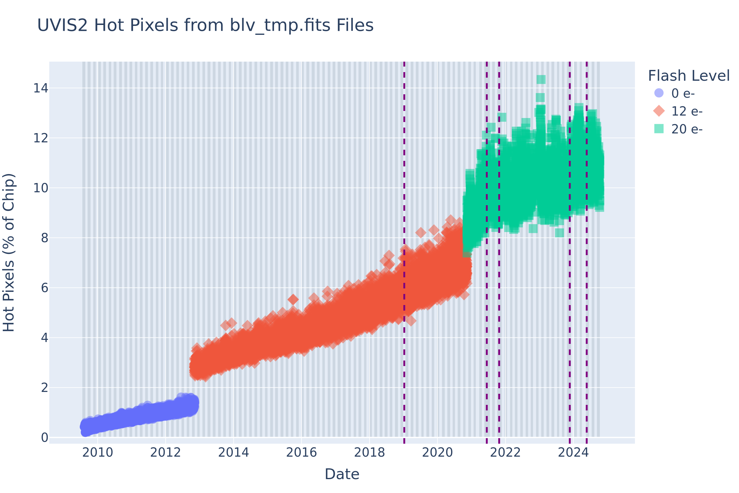
Figure 5.14: Hot pixel growth for the WFC3/UVIS CCD 2 detector between anneals from June 2009 to October 2024, as measured from CTE-corrected darks ("blc_tmp" FITS files). Points are color-coded by post-flash levels for UVIS dark frames. Light and dark gray vertical shading indicates the monthly anneal periods. Vertical dashed lines mark some of the HST safing events within the past five years.
In 2018, a detailed study of pixel behavior over time in the UVIS CCDs showed that the vast majority of hot pixels are in fact quite stable and, as such, can be calibrated (WFC3 ISR 2018-15). A small portion of pixels are genuinely unstable and should not be used; some of these are hot and unstable while others are cold and unstable. The numbers of these unstable populations (< ~1% of chip) have remained nearly unchanged over the years (Figure 5.15). To allow the pipeline to handle the distinction between stable and unstable hot pixels, the UVIS bad pixel reference file now employs the flag of 32 in the Data Quality (DQ) array to mark unstable pixels. Hot pixels continue to be assigned the usual DQ flag of 16 (Table E.3). With the additional stability DQ flag, observers have enhanced control over which pixels to include, or exclude, from their analyses.
Figure 5.15: The number of pixels (as a percentage of the detector) as a function of type: hot, cold, stable, and unstable.
![]()
5.4.10 Cosmic Rays
The fraction of WFC3 pixels impacted by cosmic rays varies from 5% to 9% per chip during 1800 sec exposures in SAA-free orbits, providing a basis for assessing the risk that the target(s) in any set of exposures will be compromised. Observers seeking rare or serendipitous objects, as well as transients, may have stringent requirements on how many cosmic rays can be tolerated in an image combination. Assuming cosmic-rays affect 5-9% of a chip in 1800 sec, at least 4-5 images will be needed to ensure that fewer than 100 pixels will be hit in all images of the combination.
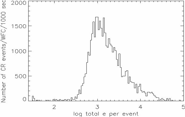
The flux deposited on a CCD from an individual cosmic ray depends less on the energy of the cosmic ray than on the distance it travels in the silicon substrate i.e. its direction of incidence. The electron deposition due to individual cosmic rays measured with ACS/WFC has a well-defined cutoff, with negligible events of less than 500 e– and a median of ~1000 e– (Figure 5.16). Similarly, the overall characteristics of the cosmic ray population appear nominal in WFC3. Miles et al. 2021 found that the rate of cosmic ray hits is ~1 hit per cm2 s-1, and a typical hit corresponds to ~2200 e–.
Figure 5.16: Electron deposition by cosmic rays on ACS/WFC.
5.4.11 Charge Transfer Efficiency
Uniform response within each pixel and excellent charge transfer efficiency (CTE) are key to achieving accurate photometric performance. CTE is a measure of how effective the CCD is at moving charge from one pixel location to the next when reading out the chip. A perfect CCD would transfer 100% of the charge as it is shunted across the chip and then out through the serial register. In practice, small traps in the silicon lattice compromise this process by retaining electrons, and then releasing them at a later time. Depending on the trap type, the release time ranges from a few microseconds to several seconds. For large charge packets (many thousand electrons), losing a few electrons along the way is not a serious problem, but for smaller signals, it can represent a substantial fraction. The UVIS CCDs are large-format devices, similar in size to those in the ACS/WFC, and thus require significantly more charge-shifting steps during readout, with more losses, than smaller devices like the STIS and WFPC2 CCDs. CTE inevitably declines over time as on-orbit radiation damage creates charge traps in the detector. Furthermore, WFC3 was installed during solar minimum, when the cosmic flux is greatest and radiation damage most rapid, so the UVIS detector experienced a steeper decline in CTE in its early years than the ACS/WFC, which was deployed at a more favorable time (Baggett et al. 2011).
Several steps were taken in the design of WFC3 to reduce CTE losses on the UVIS detector. First, shielding (similar to ACS/WFC) has been used to protect the CCDs from the high-radiation space environment, thereby slowing the production of charge traps. Second, the WFC3 CCDs have been designed with a mini-channel (improved over ACS/WFC), which reduces the number of traps seen by small charge packets during read-out transfers. Third, the detector has a charge-injection capability (not generally available for science observations - see Section 6.9.2), which inserts charge electronically in equally spaced rows of pixels to fill the charge traps (WFC3 ISR 2011-02). Fourth, an operational mode has been developed to provide controlled CCD illumination from an LED at the end of an exposure to increase the background level in the exposure. Use of this post-flash mode is now strongly recommended for observations of faint objects when the background level is expected to be less than 20 e-/pixel. The rationale for using this mode was presented in MacKenty and Smith (2012). The state of the UVIS detector’s CTE at that time is also discussed in Baggett et al. (2012). Given the current state of the CTE losses, the optimal background level (sky plus dark current plus post-flash if needed) is now 20 e-/pixel (see Section 6.9.2).
CTE is typically measured as a pixel-transfer efficiency, and would be unity for a perfect CCD. One way to measure CTE is via the Extended Pixel Edge Response (EPER) method, where a specialized readout takes flat-field exposures with a significant amount of overscan. Inefficient transfer of electrons in such exposures produces an exponential tail of charge into the overscan region. Analysis of EPER monitoring observations from 2009 through May 2020 showed a roughly linear decline of CTE over time (WFC3 ISR 2020-06). As expected, the EPER results show that the CTE has continued to decline with time and is steeper for the fainter signal levels. In addition, the trend of the linear fit residuals for the lowest EPER level show a periodicity which is anti-correlated with sunspot counts, i.e. solar activity (see Figure 5.17) This was not unexpected, given that the strength of the South Atlantic Anomaly, a region particularly damaging to instruments and through which HST must regularly pass, is also anti-correlated with the solar cycle.
Figure 5.17: Decline of EPER CTE over time in years as a function of illumination level (electrons) with over-plotted linear fits. Periodic deviations from the fits are anti-correlated with solar activity.
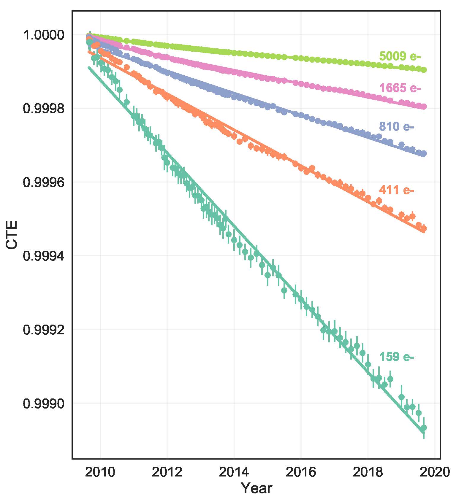
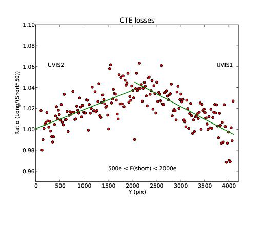
Figure 5.18: Normalized ratio of stellar fluxes measured in a long exposure of NGC 1850 to fluxes measured in a short exposure, shown as a function of Y position on the detector. Positions of 0 and 4096 reflect the location of the readout amplifiers. The ratio deviates from 1 due to the relatively greater CTE losses in the shorter (fainter) exposure.
5.4.12 Crosstalk
Crosstalk, a type of electronic ghosting, is common in devices where two or more quadrants are read out simultaneously. Both the UVIS and IR channel exhibit low levels of crosstalk.
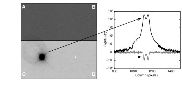
In the UVIS channel, point sources and extended targets generate low-level, negative mirror images in the quadrant adjoining the target quadrant, on the same chip (i.e., crosstalk does not cross between the chips). The crosstalk effect is linear with flux and is stronger for targets in quadrant A or C. In a full-frame, unbinned, four-amp readout with a target in quadrant A or C, the crosstalk level is ~ -2 × 10⁻⁴ that of the source; for a target in quadrant B or D, the crosstalk level is ~ -7 × 10⁻⁵ that of the source (WFC3 ISR 2012-02). To within the errors, the crosstalk due to hot pixels and cosmic rays is the same as that due to point or extended sources. Figure 5.19, from WFC3 ISR 2009-03, illustrates the crosstalk effect as observed in an image taken during instrument ground tests.
The low-level effects of crosstalk can be mitigated by dithering: the mirror image nature of the crosstalk moves the features in a direction opposite to the target motion, i.e., they will appear to be transients and thus be removed during the drizzling procedure. Alternatively, crosstalk can be removed from single images by scaling the target image quadrant by the amp-dependent factor noted above, flipping the image about the y-axis, and subtracting it from the crosstalk image quadrant.
| An IDL routine that removes crosstalk, as described in WFC3 ISR 2012-02, can be obtained from the WFC3 Crosstalk webpage along with a Python implementation of the IDL code. |
Figure 5.19: Crosstalk test frame (left), and 20-line average cuts through the target and crosstalk images (right). The image is displayed with a hard inverted greyscale stretch. The target was placed in quadrant C, and the crosstalk appears in quadrant D. The faint large ring in C offset from the primary target is an optical window ghost.
-
WFC3 Instrument Handbook
- • Acknowledgments
- Chapter 1: Introduction to WFC3
- Chapter 2: WFC3 Instrument Description
- Chapter 3: Choosing the Optimum HST Instrument
- Chapter 4: Designing a Phase I WFC3 Proposal
- Chapter 5: WFC3 Detector Characteristics and Performance
-
Chapter 6: UVIS Imaging with WFC3
- • 6.1 WFC3 UVIS Imaging
- • 6.2 Specifying a UVIS Observation
- • 6.3 UVIS Channel Characteristics
- • 6.4 UVIS Field Geometry
- • 6.5 UVIS Spectral Elements
- • 6.6 UVIS Optical Performance
- • 6.7 UVIS Exposure and Readout
- • 6.8 UVIS Sensitivity
- • 6.9 Charge Transfer Efficiency
- • 6.10 Other Considerations for UVIS Imaging
- • 6.11 UVIS Observing Strategies
- Chapter 7: IR Imaging with WFC3
- Chapter 8: Slitless Spectroscopy with WFC3
-
Chapter 9: WFC3 Exposure-Time Calculation
- • 9.1 Overview
- • 9.2 The WFC3 Exposure Time Calculator - ETC
- • 9.3 Calculating Sensitivities from Tabulated Data
- • 9.4 Count Rates: Imaging
- • 9.5 Count Rates: Slitless Spectroscopy
- • 9.6 Estimating Exposure Times
- • 9.7 Sky Background
- • 9.8 Interstellar Extinction
- • 9.9 Exposure-Time Calculation Examples
- Chapter 10: Overheads and Orbit Time Determinations
-
Appendix A: WFC3 Filter Throughputs
- • A.1 Introduction
-
A.2 Throughputs and Signal-to-Noise Ratio Data
- • UVIS F200LP
- • UVIS F218W
- • UVIS F225W
- • UVIS F275W
- • UVIS F280N
- • UVIS F300X
- • UVIS F336W
- • UVIS F343N
- • UVIS F350LP
- • UVIS F373N
- • UVIS F390M
- • UVIS F390W
- • UVIS F395N
- • UVIS F410M
- • UVIS F438W
- • UVIS F467M
- • UVIS F469N
- • UVIS F475W
- • UVIS F475X
- • UVIS F487N
- • UVIS F502N
- • UVIS F547M
- • UVIS F555W
- • UVIS F600LP
- • UVIS F606W
- • UVIS F621M
- • UVIS F625W
- • UVIS F631N
- • UVIS F645N
- • UVIS F656N
- • UVIS F657N
- • UVIS F658N
- • UVIS F665N
- • UVIS F673N
- • UVIS F680N
- • UVIS F689M
- • UVIS F763M
- • UVIS F775W
- • UVIS F814W
- • UVIS F845M
- • UVIS F850LP
- • UVIS F953N
- • UVIS FQ232N
- • UVIS FQ243N
- • UVIS FQ378N
- • UVIS FQ387N
- • UVIS FQ422M
- • UVIS FQ436N
- • UVIS FQ437N
- • UVIS FQ492N
- • UVIS FQ508N
- • UVIS FQ575N
- • UVIS FQ619N
- • UVIS FQ634N
- • UVIS FQ672N
- • UVIS FQ674N
- • UVIS FQ727N
- • UVIS FQ750N
- • UVIS FQ889N
- • UVIS FQ906N
- • UVIS FQ924N
- • UVIS FQ937N
- • IR F098M
- • IR F105W
- • IR F110W
- • IR F125W
- • IR F126N
- • IR F127M
- • IR F128N
- • IR F130N
- • IR F132N
- • IR F139M
- • IR F140W
- • IR F153M
- • IR F160W
- • IR F164N
- • IR F167N
- Appendix B: Geometric Distortion
- Appendix C: Dithering and Mosaicking
- Appendix D: Bright-Object Constraints and Image Persistence
-
Appendix E: Reduction and Calibration of WFC3 Data
- • E.1 Overview
- • E.2 The STScI Reduction and Calibration Pipeline
- • E.3 The SMOV Calibration Plan
- • E.4 The Cycle 17 Calibration Plan
- • E.5 The Cycle 18 Calibration Plan
- • E.6 The Cycle 19 Calibration Plan
- • E.7 The Cycle 20 Calibration Plan
- • E.8 The Cycle 21 Calibration Plan
- • E.9 The Cycle 22 Calibration Plan
- • E.10 The Cycle 23 Calibration Plan
- • E.11 The Cycle 24 Calibration Plan
- • E.12 The Cycle 25 Calibration Plan
- • E.13 The Cycle 26 Calibration Plan
- • E.14 The Cycle 27 Calibration Plan
- • E.15 The Cycle 28 Calibration Plan
- • E.16 The Cycle 29 Calibration Plan
- • E.17 The Cycle 30 Calibration Plan
- • E.18 The Cycle 31 Calibration Plan
- • E.19 The Cycle 32 Calibration Plan
- • E.20 The Cycle 33 Calibration Plan
- • Glossary